find av if vin is 3.5 vp - p with an internal resistance of 3 kohms, vcc is 11 volts, r1 is 1.0 kohms, r2 is…
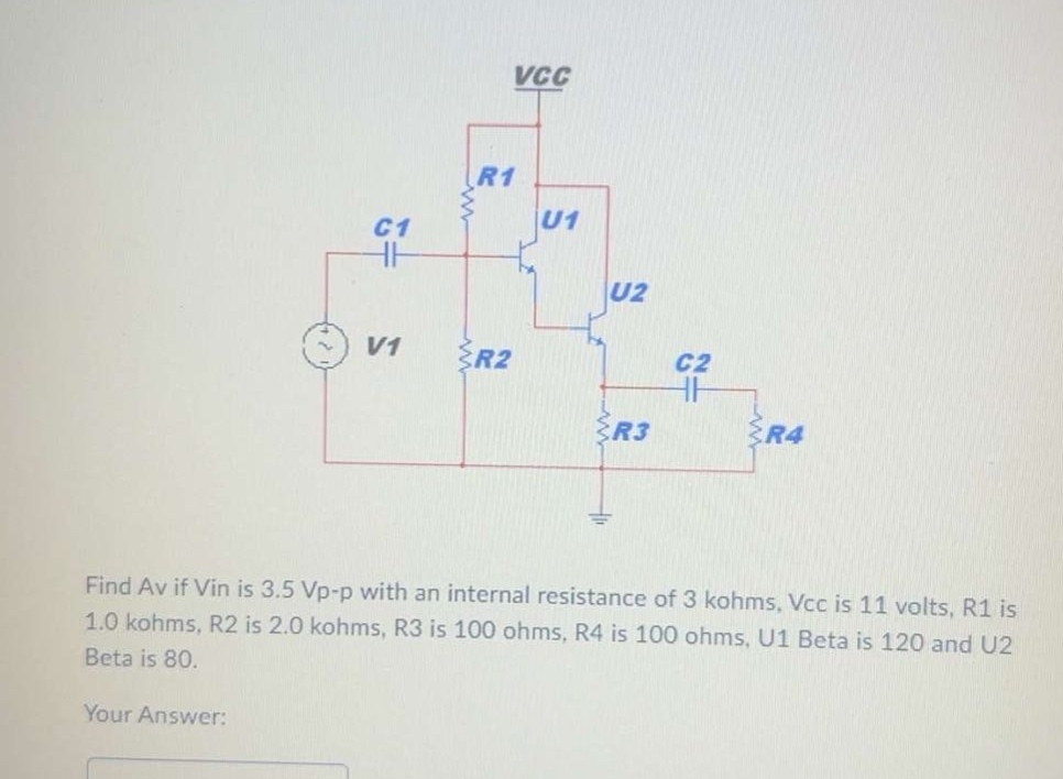
find av if vin is 3.5 vp - p with an internal resistance of 3 kohms, vcc is 11 volts, r1 is 1.0 kohms, r2 is 2.0 kohms, r3 is 100 ohms, r4 is 100 ohms, u1 beta is 120 and u2 beta is 80. your answer:
Answer
Explanation:
Step1: Calculate input - stage parameters
First, find the input - stage base - current and voltage - gain. For the first transistor U1, assume the input resistance of the base - emitter junction $r_{\pi1}=\beta_1\frac{V_T}{I_{C1}}$. But we can also use the small - signal analysis in a simplified way. The input resistance of the first stage $R_{in1}=R1\parallel R2$. $R_{in1}=\frac{R1\times R2}{R1 + R2}=\frac{1000\times2000}{1000 + 2000}=\frac{2000000}{3000}\approx666.67\Omega$ The voltage divider formed by the internal resistance of the source $R_s = 3000\Omega$ and $R_{in1}$ affects the voltage at the base of U1. The voltage at the base of U1, $V_{b1}=\frac{R_{in1}}{R_{in1}+R_s}V_{in}$ $V_{b1}=\frac{666.67}{666.67 + 3000}\times3.5\approx0.616V_{p - p}$ The small - signal voltage gain of the common - emitter stage (U1) $A_{v1}=-\beta_1\frac{R_{C1}}{r_{\pi1}+R_{E1}}$. In a simple case, if we assume $R_{E1} = 0$ (ignoring the base - emitter resistance for a quick estimate), and $R_{C1}$ is the resistance seen at the collector of U1. The collector of U1 is connected to the base of U2. The equivalent resistance at the collector of U1 looking into U2 is approximately $r_{\pi2}=\beta_2\frac{V_T}{I_{C2}}$. A more practical way is to consider the current gain. The current gain of U1 is $\beta_1 = 120$. The output of U1 is connected to the input of U2. The input resistance of U2 is $R_{in2}=r_{\pi2}=\beta_2\frac{V_T}{I_{C2}}$. Assuming a DC - bias analysis first, we can also use the small - signal model. The voltage gain of the first stage $A_{v1}=-\beta_1\frac{R_{L1}}{r_{\pi1}}$, where $R_{L1}$ is the load resistance of U1 which is $R_{in2}$.
Step2: Calculate second - stage parameters
For the second transistor U2, the input resistance $R_{in2}$ is considered. The small - signal voltage gain of the common - emitter stage (U2) $A_{v2}=-\beta_2\frac{R_{L2}}{r_{\pi2}+R_{E2}}$, where $R_{E2}=R3$ and $R_{L2}=R4$. $A_{v2}=-\beta_2\frac{R4}{r_{\pi2}+R3}$ Assuming $r_{\pi2}\gg R3$ (a common approximation in small - signal analysis for a well - biased transistor), $A_{v2}=-\beta_2\frac{R4}{R3}$ Substituting $\beta_2 = 80$, $R3 = 100\Omega$ and $R4 = 100\Omega$, we get $A_{v2}=- 80$ The overall voltage gain $A_v=A_{v1}\times A_{v2}$ Another way: The overall small - signal voltage gain of the two - stage amplifier can be calculated using the formula for a cascade of common - emitter amplifiers. The input resistance of the first stage $R_{in}=R1\parallel R2$. The overall voltage gain $A_v=-\frac{\beta_1\beta_2R4}{(R1\parallel R2)}$ $A_v=-\frac{120\times80\times100}{\frac{1000\times2000}{1000 + 2000}}$ $A_v=-\frac{120\times80\times100\times3000}{1000\times2000}$ $A_v=-144$
Answer:
$- 144$